Back in the late 80s and early 90s, when the Amiga was relevant as a technical revolution, I was never able to lay my hands on anything beyond an 68000 with 7.14MHz. Years later, around 1997, I acquired an Amiga 3000 with 25MHz as part of one of my university side gigs of porting software from various UNIXes (in this case SCO Unix) to Linux. But a 040 or even 060 was far out of reach until I was well into my first full time job at SUSE Linux when I got a Cyberstorm MK1 that – as we know – doesn’t fit into the A3000. Long story short, the first time I actually ever ran an Amiga with something faster than the 68030 @ 25 was around …. Christmas 2019.
As life happens, and we sometimes overcompensate for our youth’s desires as we grow older, I added one of Chucky’s A3660 rev 1.1 to my collection, (built by Nicolas Baumgardt who lives in Switzerland, but only few miles from where I grew up and hacked on the Amiga back in 1987) that so far consisted of the A3640 that screamed for pad replacements and recaps.
Along the way I learned that the Amiga CPU local bus is really a 68030 bus, so memory access on everything above a 030 has to be translated and is then slightly slower than with an actual 68030. Ouch.
I also learned that the Zorro III slot is not really all that great. Well, Super Buster is not in its current implementation. While the theoretical maximum of Zorro III beats the first PCI standard, the actual implementation is stuck at 8-10MB/s memory access speed. We need an update Dave Haynie! Then our BigRAM+es could be really super awesome!
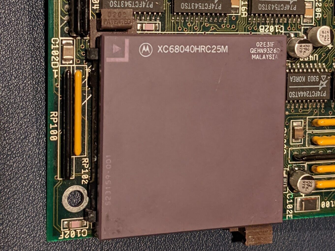
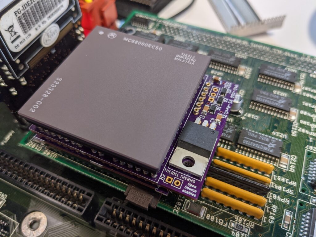
But back to … back to the 68060. Once I tasted the sweet excess of the Motorola flagship’s raw CPU power, and when I got my beautiful Hakko soldering station, I had to upgrade my 3640 to a 060 processor as well.
To do that, you need an adapter that converts from one CPU pinout to the other (similar to the overdrive CPUs in the 90s)
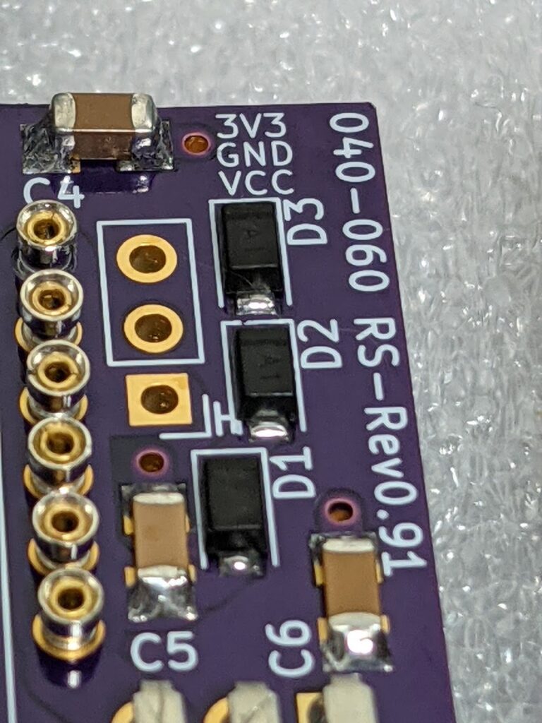
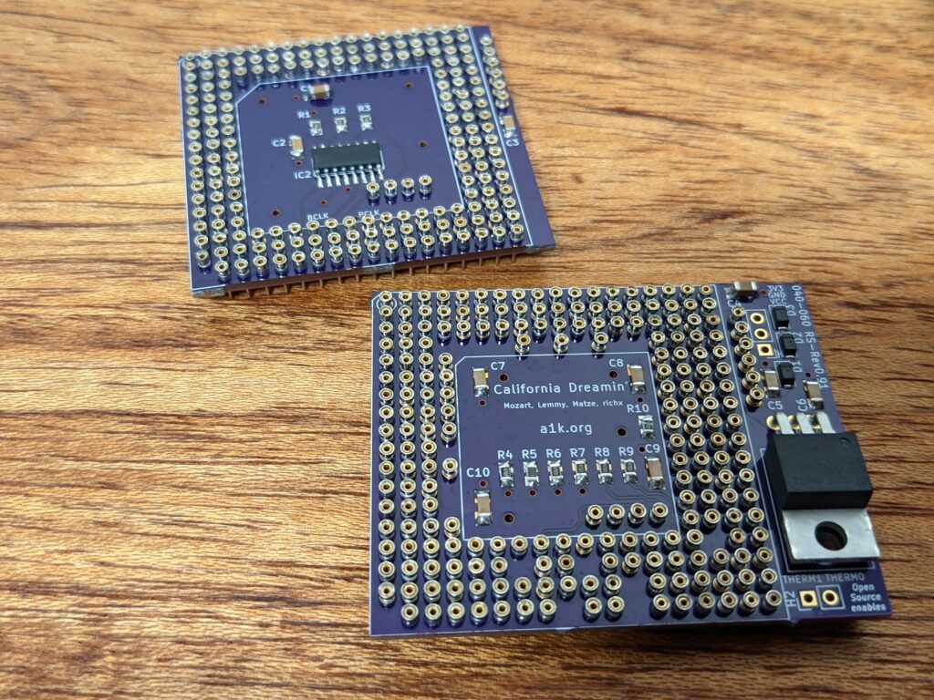
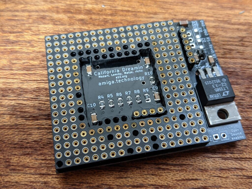
And here comes the journey. I did make the mistake (a beautiful purple mistake) of ordering three PCBs for the a1k.org 68040 to 68060 adapter from OSHpark for USD43. As I found out later, PCBway would only charge me USD5 for 10 PCBs.
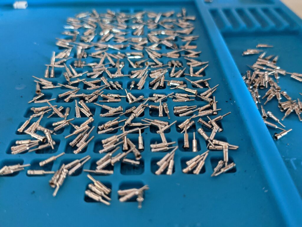
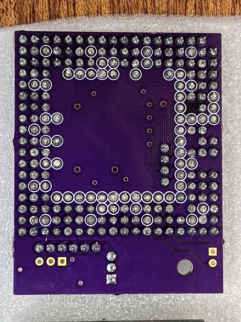
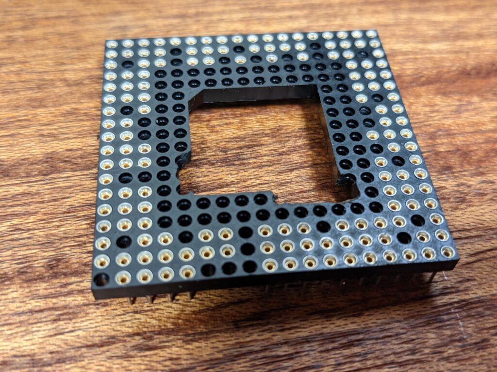
The assembly is a game of patience. Because I had the PCBs produced with the standard width of 1.6mm it was unfeasible to solder on 68040 or 68060 sockets onto them. So off to Ebay to grab pin headers and extract the pins from them, as there does not seem to be a place that sells pins at a reasonable price.
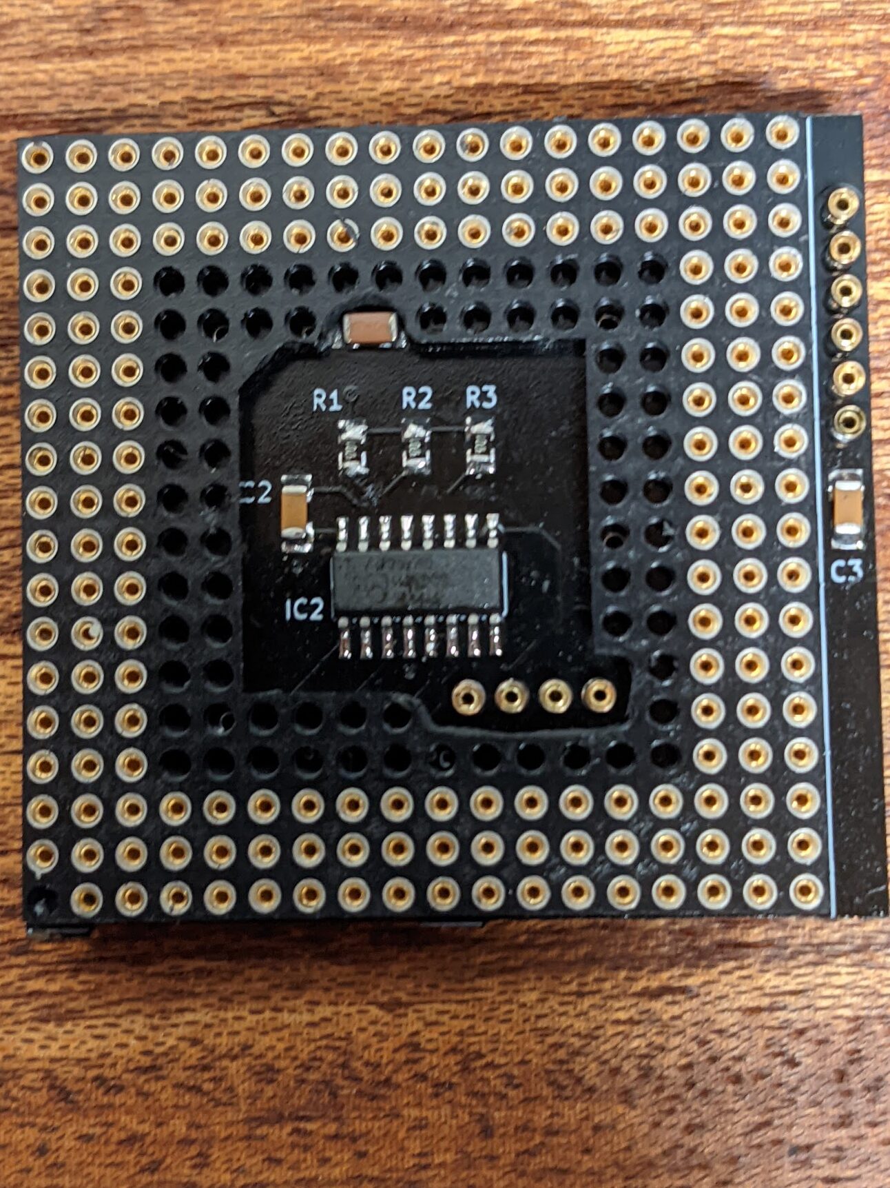
The whole concoction consists of two boards, the 68040 part and the 68060 part. The top part converts the current from 5V to 3V. Since most pins are identical on both processors, they are directly passed through between the two boards. Not all of them, however, and these pins will have to be cut on the top board. The PCB I used had little circles around the pins that needed cutting, to make the process almost fool-proof.
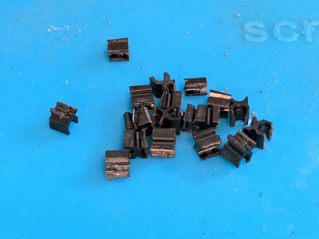
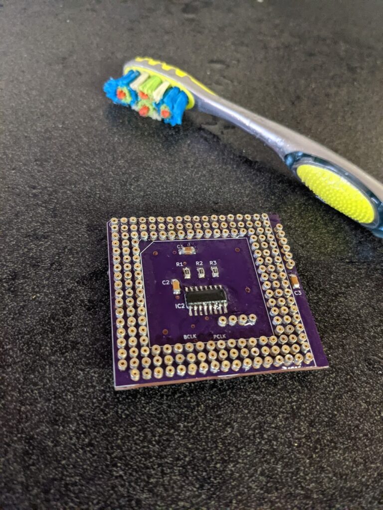
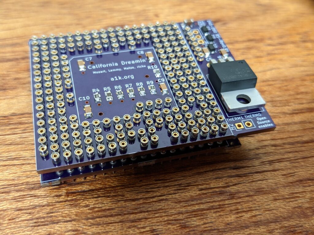
To keep the pins from falling out, or from slightly shifting when soldering, I used a 68040/060 socket on top to hold them in place. I also soldered one line of pins at a time, and cut the pins right after finishing each line, as this would get to be a nightmare, as XXXXXX (name redacted) a dear friend of mine had to find out shortly before dumping his version of the adapter into the trash 🙂
Now I always prefer SMD components to through hole stuff, but in this case the through hole portion is mind bendingly annoying. Mind you, it requires soldering about 400 pins in a very tight space. It is very easy to either use too much or too little solder, keeping the pins wiggling or put solder on the tip of the pins, which will need annoying reworks later as the whole thing is a tight, tight fit. Nothing that can’t be solved with overzealous flux use.
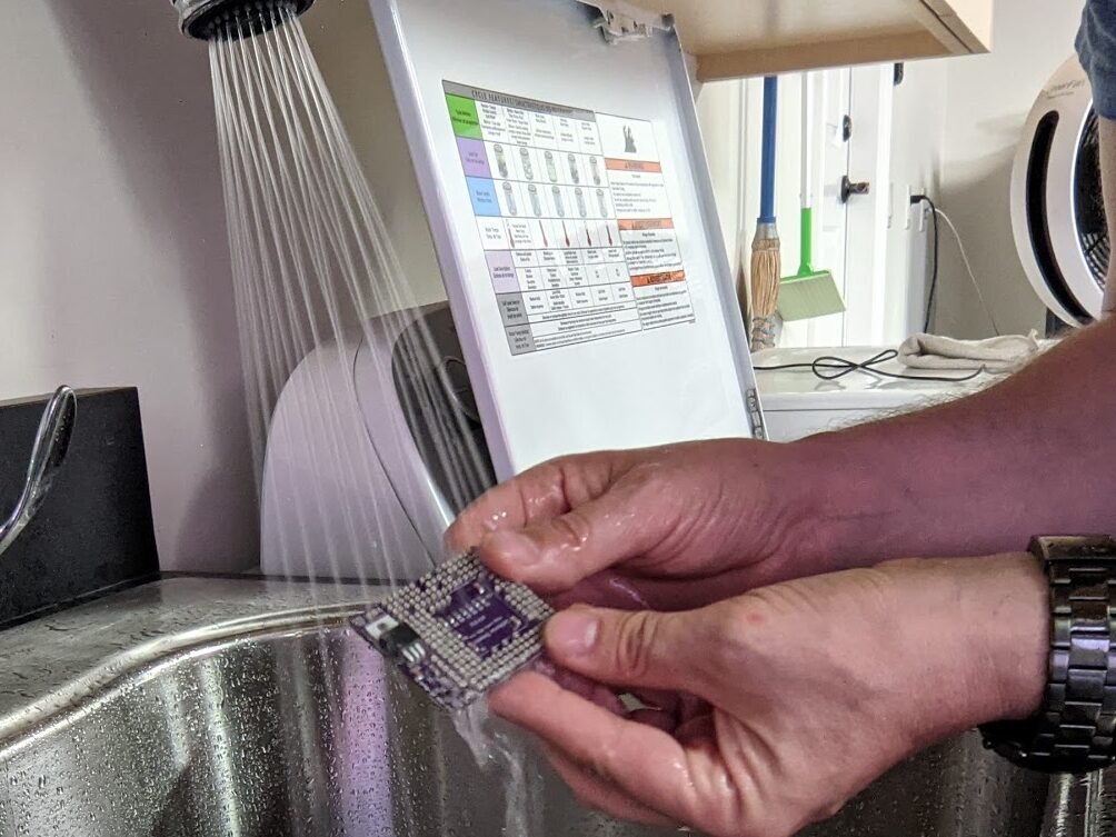
Last, bring out the toothbrush and the flux remover, and give both parts a good rub, and it’s time for a test.
Yippie! It works.
As I had another PCB and the project seemed easy enough, I sold the first version on Ebay after several hours of testing and started working on the second one. This one is completely assembled, but after all this time still not working. The story continues….
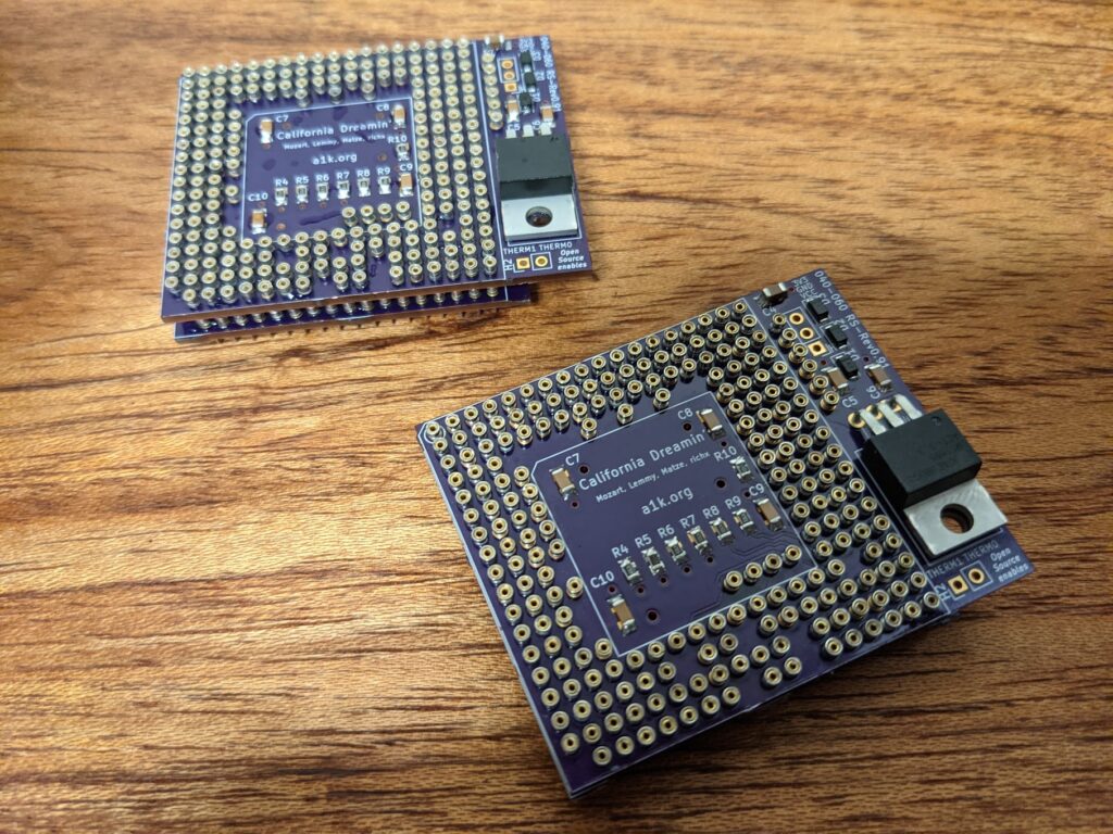
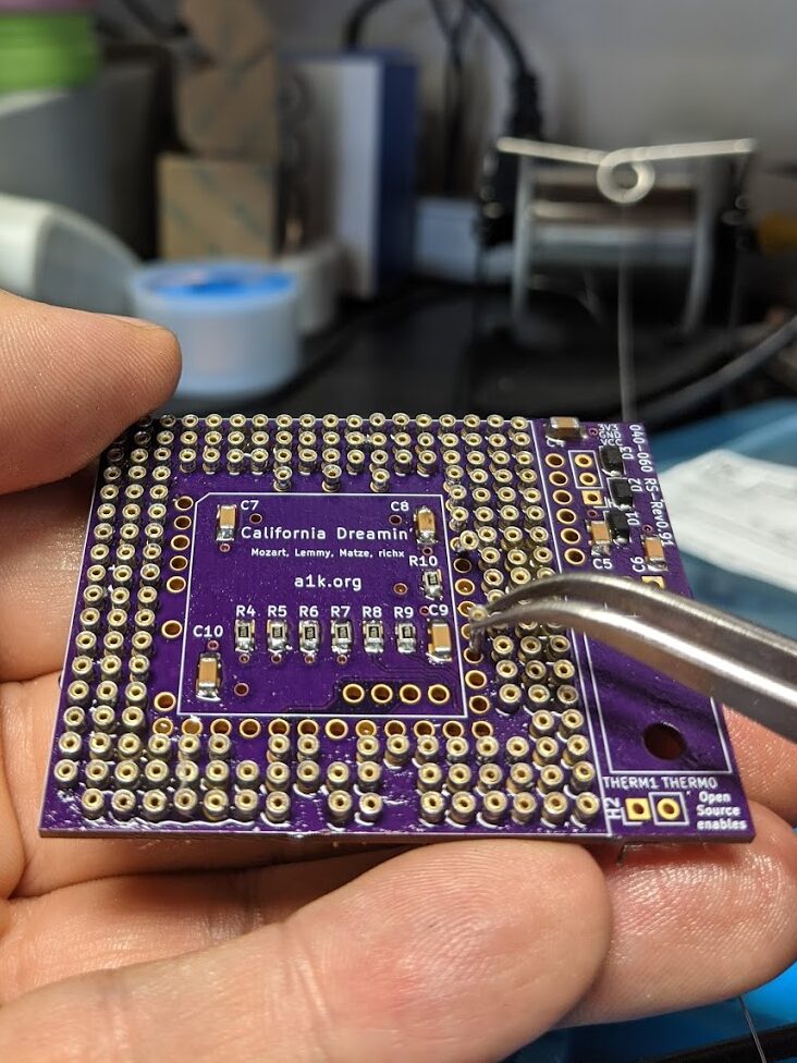
I also got another batch of sockets and PCBs… This time I made the PCBs 0.8mm thick (half the normal size), so I can just use normal PGA sockets instead of going down the pin craziness again.
But even now, things are not as easy as I had hoped. Turns out, my sockets have 5 rows of substrate, of which the 68040 uses 3 and the 68060 uses 4. Unfortunately the PCB design places some components right under the inner substrate and the 10uF caps I am using are just a tad too high.
No problem! That’s what dremels are for.
My fellow Amigan Adam Polkosnik suggested to use an intermediate socket to avoid cutting the pins all together. That makes for a nice and clean solution and cuts some build time off the adapter too. Very elegant and clever.
And along the way I ran out of diodes to build the next adapter. I hope that having a third adapter will allow me to debug which of the two halves of my second adapter is buggy.
To be continued…
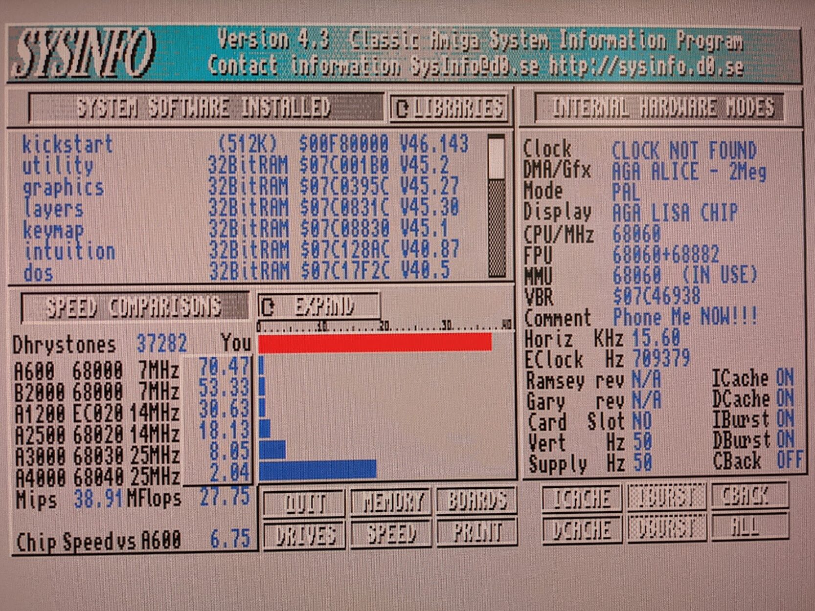
Reminder: If you are using a 68060 CPU with FPU on your Amiga you will need a patched kickstart if you are on 3.1 or earlier, or upgrade to at least 3.1.4.
You mean, if you do it this way, that is, by upgrading a ‘040 CPU card to a ‘060 one via a socket adapter. Regular ‘060 cards – which were designed to work with a ‘060 – of course handle transparently (they have their own ROM usually, which does the dirty work), and can work with basically any Kickstart version – of course using KS1.3 with a ‘060 is not very rewarding… 🙂 Just as a clarification. Great post, btw!
Hi Stefan,
Will doing a bit of web digging, came across your guide here. Read where you mentioned selling your first unit on eBay, and think i was the buyer 🙂
This unit was assembled with the regulator “tethered” to the adapter. Sure looks the same otherwise, and am not going to risk disassembly to find out.
Intended use here is with an Atari Clone application.
Just now getting around to reinstalling the 68040 CPU expansion board for the machine, and soon will be testing the adapter.
The existing board utilizes an MC88915 FN100 for the 040 clock driver. Don’t have the drawings for this adapter, is the smt on this pcb the 060 clock driver (88917LV?).
If so, thinking I’ll have to reconfigure how the main board clock is passed to the 040 socket. I know it’s currently “wired” to only provide a 2X clock to the CPU.
Going to have to look up the hot air station you purchased, sure looks easier than using a propane torch on the poor old Atari 🤣
Cheers,
Mike
Interesting tidbit, my son works at Stanford University Children’s Hospital, recently moved from Mountain View to, you guessed it, Sunnyvale, Atari city 🙂
Hi Michael, I was just going to check to make sure but eBay does not seem to let me go back that far. My soldering definitely got better, but I had tested the one I sold on on eBay extensively before putting it up. Let me know how it works for you! The one I sold is the one you see in the picture “The final product” above. Any feedback is welcome!
Depending on the clock rate of your 040 and the revision of the 060 you want to use, you might have to make adjustments, but generally the 040 splits the clock it gets in half (i.e. 50MHz oscillator means 25MHz CPU clock), so if you replace a 25MHz 68040 you will automatically see your 060 be clocked at 50MHz. How high you can actually go depends a lot on the individual CPU. I have a revision 6 060 running at 100MHz (but I had to exchange the voltage regulator with a 3.6V model for it to be stable)
For the hot air station I am using a Quick 861DW. Before that I had a knock off 858D that I bought for roughly 40 bucks. It worked fine for the occasional use.
… It is a small world! Make sure to say hi if you’re ever in the area.
Hi Stefan,
Broke down and sperated to two halves. I don’t think this unit one you sold.
Been reading until my eyes bleed numerous Amiga archives. The only thing that stands out, something I’d missed years before, are some of the Amiga cards have jumpers which enable/disable which pin on the 060 the 040 BCLK goes to, as well as pulling the unused 060 clock pin to ground.
This adapter routes BCLK to CLKEN. This as I understand allows for 1/2 speed bus clock.
The 040 (88915) is setup to sync off the 16MHz expansion bus, feed 32MHz to Q outputs and provide 2XQ to PCLK for the 040 card.
However, CLK on the 060 is left floating on this adapter.
You think this an issue?
Another Atari 060 (working 🙂 ) accelerator operates the bus at full speed, with schematics showing CLKEN tied to ground.
About the only reference to this I’ve seen was buried deep in discussions back in the early 2000’s where Amiga users were first using the adapters on 040 machines.
Came across some other interesting mods where a group member has come up with some logic allowing more timing windows (TA, TS, ect) that helped when boosting the 040 above 40MHz. Oddly enough also have a couple of Quad Doubler for Apples, and read where they were drop in on some of the Amiga boards.
Had this ever been tested or could possibly work on a 040 Mac?
Apologies for the late reply here. I don’t have a Mac to try it with, but chances are it will need some sort of software patches in addition to the adapter.